What is PCB potting and why it is used
What is PCB potting and why it is used
PCBs, an abbreviation for printed circuit boards, are vital components installed in modern electronics. These circuits help to transfer signals between various components and act as a bridge to connect various electronic components. To make sure that PCB acts optimally you need to protect it from harsh environments such as exposure to chemicals, moisture, or physical stress. You certainly cannot eliminate these harsh environmental conditions but what you can do is to shield the sensitive circuit with a potting compound to protect it from the harmful effects of such environmental conditions.
PCB is a critical technique that can safeguard your sensitive and vital electronic components from harmful environmental effects. Let us take a deep look at what is PCB potting and check out its uses/applications in the world of electronics.
 What is PCB potting?
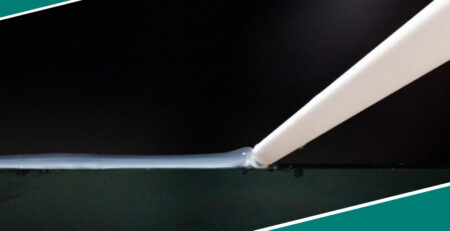
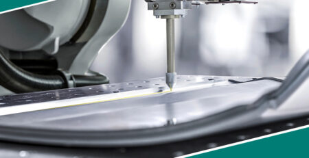
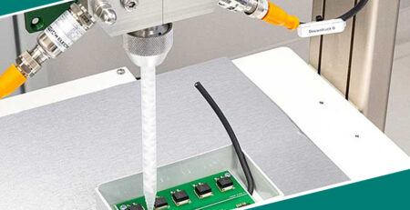
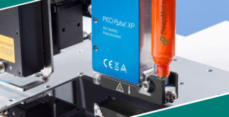
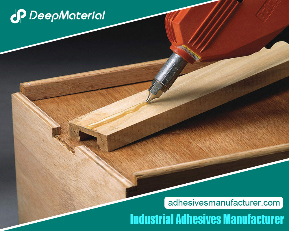
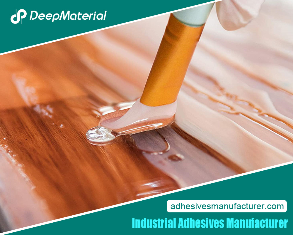
PCB potting is a protective layer that is encapsulated over the PCB to protect the delicate circuitry against environmental hazards, chemical exposure, excessive heat, and physical impacts. PCB potting is also known as potting compound application or encapsulation so if someone refers to it with these names then do not get confused.
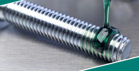
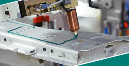
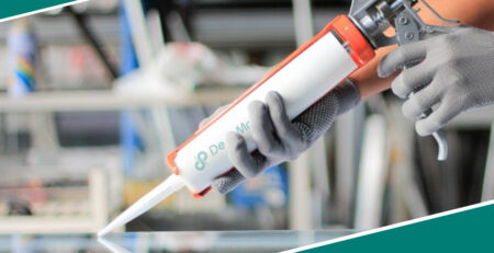
The potting compound used for PCBs is usually an epoxy or resin. You can encapsulate PCB with this potting compound by filling the enclosures with it which will then protect the entire board. You can also inject or pour it around the PCB into a mold that encapsulates the entire structure and serves as a protective shield.
Now that you are aware of what is PCB potting, let us move to the critical question of why we use this potting as a safeguard layer.
Why PCB potting is used?
Here are the reasons that require the usage of PCB potting.
- Protection against the environment: PCBs can get damaged from harsh environmental effects such as dust, moisture, chemicals, and other harmful factors. Potting component shields the electronic components and circuits from these harmful effects by shielding the ingress of contaminants and moisture inside the circuit that can damage the components and disrupt their working. By offering a protective layer, potting can work as a resistance against environmental effects and corrosion. Potting is critically useful in applications when the PCB is exposed to harsh conditions, for instance when it is placed in automotive systems (subject to vibrations), outdoors (where chances of moisture exposure are increased), and in industrial machinery (where the chances of physical impact and chemical exposure are paramount).
- Mechanical stability: Mechanical stability is of utmost importance to protect the components of PCB. It offers a mechanical reinforcement to the sensitive components inside circuits minimizing the risk of degradation or failure from shock, vibration, and physical impact. Potting is useful in distributing the mechanical stress evenly across the circuit enhances reliability and ensures the durability of the components and the circuit as a whole. In addition, it also takes care of the wire pairing that can occur when PCB case and PCB’s vibrations occur together and enhance the stress on components that can lead to early component failure. Potting works to make the PCB resistant against such vibration pairs and enhance the level of stress.
- Enhanced performance: With environmental exposure without protection, the performance of components and the overall circuit can get compromised. Potting is useful in enhancing the electronic performance of PCBs. It protects the circuit from tampering, voltage leaks, and moisture ingress which can lead to optimal performance. It also enhances performance by protecting the circuit against early system failure, unintended connection building, and wiring disconnections.
- Electric insulation: Potting compounds have electric insulation features which is why they can help you protect the PCB against electrical failures and short circuits. Potting is useful in that it shields the conductive components and traces. This way it lowers the possible risk of arcing, electrical inference, and voltage leaks. By providing electrical insulation, potting enhances the safety of PCBs.
- Management of thermal flow: Potting compounds used to encapsulate PCB usually have good thermal conductivity. They help them to efficiently dissipate heat from the electronic components of PCB. This efficient heat dissipation helps to maintain the optimal temperature required for ideal operations of PCB. It helps to alleviate the lifespan of components and ensure that the circuit performs optimally without any disruption. Potting is of paramount use when PCB is placed in an environment where the temperature remains quite high or under heavy load.
- Protection against overheating: Dirt and dust can enter the PCB units and cause overheating which can affect the functionality of delicate components and can even lead to component failure. Potting can save you from the risk of overheating and signal interference by building a protective layer outside the PCB to prevent the entry of dust and dirt.
- Enhances privacy: PCB potting works as an added layer of privacy and security for your system. Potting provides an outer encapsulation that makes it difficult to access the electronic device and prevents the chances of reverse engineering. This way it can enhance the security and privacy of your PCB device.
- Resistance against corrosion: PCB potting offers great resistance against corrosion by protecting the metallic components through a protective shield. It prevents moisture infusion and resistance against corrosive chemicals and humidity.
- Sealing: PCB potting is of utmost use as it protects all components from all types of contaminants. Many PCB users think that if they keep the PCB device in a safe place away from contaminants then they do not require potting encapsulation. However adequate sealing offers protection beyond the calculated risks. It helps to safeguard PCBs from tampering, accidental contact, or unauthorized access. This feature makes potting extremely useful and necessary for PCB devices.
- Alternative to conformal coating: Traditionally, conformal coating is used to protect PCBs from environmental effects. In contrast to conformal coating, potting offers comprehensive protection to PCB by encapsulating it entirely and safeguarding all components. The importance of PCB potting cannot be denied especially when a higher level of protection is required against harsh environmental impacts.
For more about what is PCB potting and why it is used, you can pay a visit to Deepmaterial at https://www.adhesivesmanufacturer.com/ for more info.