Epoxy Underfill Encapsulant

As the world of microelectronics advances with ever-shrinking components and intricate designs, the need for robust protection and reliable performance has become paramount. Epoxy underfill encapsulant, a cutting-edge solution, has emerged as a key player in safeguarding delicate electronic components from mechanical stresses, thermal cycling, and environmental factors. By filling the gaps between microchips and substrates, epoxy underfill encapsulant significantly enhances mechanical integrity and thermal conductivity. This comprehensive exploration delves into the realm of epoxy underfill encapsulant, uncovering its composition, applications, benefits, and its role in shaping the future of microelectronics.
Introducing Epoxy Underfill Encapsulant
We are thrilled to introduce our latest technological advancement – the Epoxy Underfill Encapsulant. This state-of-the-art solution, engineered to redefine electronic packaging standards, promises to revolutionize how we protect and enhance electronic devices.
At its core, the designers have crafted the Epoxy Underfill Encapsulant to address the challenges of modern electronics, offering a reliable barrier against physical and environmental stressors. Seamlessly filling gaps and voids within intricate components fortifies the structural integrity of devices, safeguarding them against mechanical shocks, vibrations, and moisture ingress.
One of the standout features of this encapsulant is its exceptional thermal conductivity. As electronic devices continue to push performance boundaries, heat management becomes paramount. Our Epoxy Underfill Encapsulant excels in dissipating heat efficiently, preventing overheating, and ensuring optimal functioning even under demanding conditions.
Beyond its technical prowess, the encapsulant boasts remarkable versatility. It adapts seamlessly to various applications, from microelectronics to circuit boards, offering consistent and uniform coverage. Its user-friendly viscosity ensures hassle-free integration into manufacturing processes, saving time and resources.
Moreover, the Epoxy Underfill Encapsulant demonstrates a commitment to environmental sustainability. Formulated with eco-friendly materials, it aligns with our mission to reduce our ecological footprint without compromising performance.
In a world where innovation drives progress, the Epoxy Underfill Encapsulant stands at the forefront, a testament to our dedication to engineering solutions that empower the future of electronics. Welcome a new era of reliability, durability, and efficiency with our groundbreaking Epoxy Underfill Encapsulant.
Importance of Microelectronics Packaging
In the realm of advanced technology, microelectronics packaging emerges as a critical facet that significantly influences electronic device performance, durability, and reliability. This packaging is the protective shield, ensuring the intricate components remain operational under various conditions. Here’s why microelectronics packaging holds immense significance:
- Component Protection:Microelectronics packaging provides a barrier against external elements like dust, moisture, and contaminants that can compromise the sensitive components’ functionality. It shields delicate parts from mechanical stresses, temperature fluctuations, and physical damage during handling and transport.
- Thermal Management:With electronic devices becoming more compact and powerful, efficient thermal management is paramount. Packaging designs with proper heat dissipation properties help prevent overheating, ensuring devices operate optimally and maintain longevity.
- Signal Integrity:Effective packaging minimizes electromagnetic interference and cross-talk between components, preserving signal integrity and data transmission accuracy. Properly designed packages maintain the electrical performance of components, which is vital for high-speed communication and processing.
- Miniaturization and Integration:Microelectronics packaging enables the integration of multiple components into smaller form factors. This miniaturization is essential for modern gadgets, allowing sleek designs while maintaining high functionality.
- Reliability and Longevity:Well-designed packaging enhances electronic devices’ overall reliability and lifespan. It safeguards against harsh environments, shocks, and vibrations, ensuring devices perform consistently over time without frequent failures.
- Manufacturing Efficiency:Packaging facilitates streamlined manufacturing processes by enabling automation and reducing manual labor. Efficient packaging designs lead to higher yield rates, reduced production costs, and faster time-to-market.
- Environmental Considerations:Sustainable packaging materials and designs can contribute to minimizing electronic waste. Environmentally conscious packaging solutions align with global efforts to reduce the environmental impact of electronic devices.
Microelectronics packaging is not merely an afterthought but a critical component that underpins electronic devices’ functionality, longevity, and efficiency. Its role in safeguarding components, managing heat, preserving signal integrity, and promoting sustainability is integral to modern technological advancements.
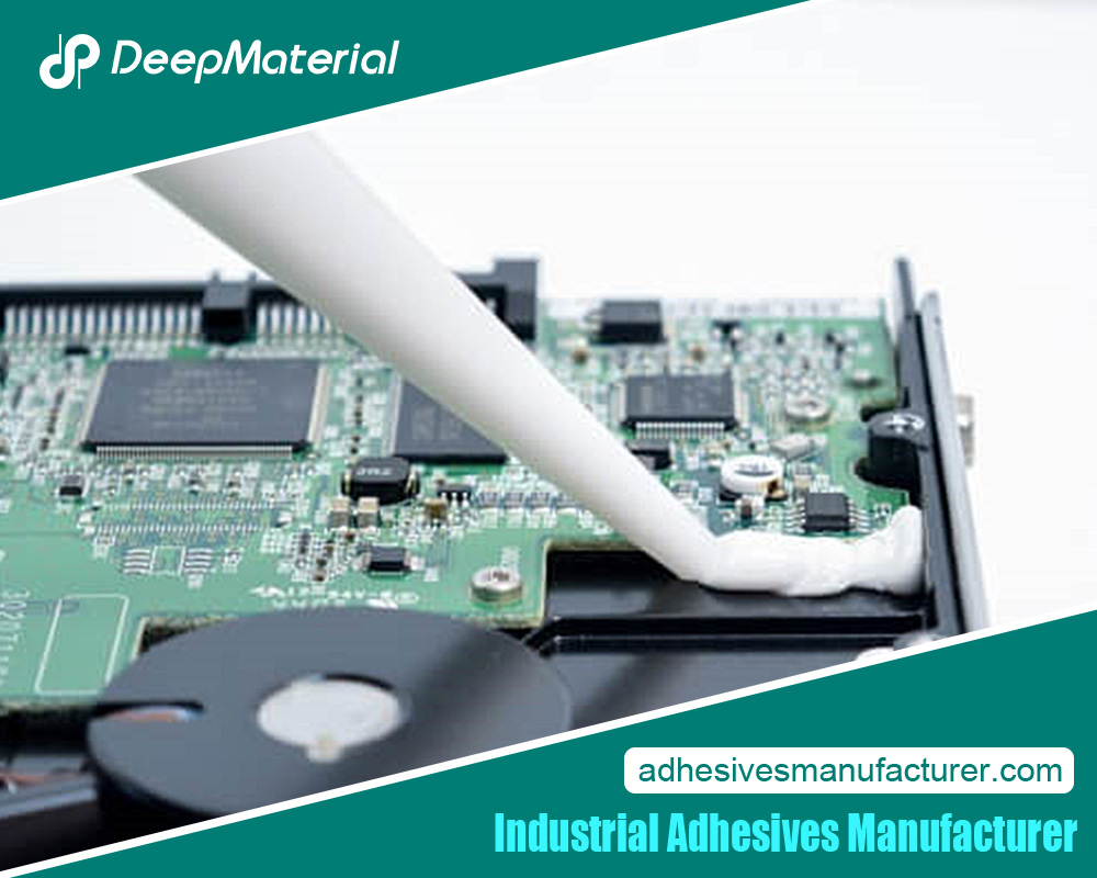
Function of Underfill Encapsulants
Underfill encapsulants play a pivotal role in ensuring the reliability and longevity of electronic assemblies, particularly in microelectronics and semiconductor packaging. Designers craft these specialized materials to fill the gap between semiconductor chips and their substrates, enhancing mechanical stability and protecting delicate components. Here are the critical functions of underfill encapsulants:
- Stress Relief:Underfill encapsulants relieve the stress due to the differences in thermal expansion coefficients between the semiconductor chip and the substrate. Minimizing the impact of temperature changes lowers the likelihood of cracks and malfunctions.
- Enhanced Bonding:Underfill materials provide adhesive solid bonding between the chip and the substrate, preventing chip detachment due to mechanical stresses, vibrations, or environmental conditions.
- Thermal Management:Effective underfill encapsulants offer high thermal conductivity, facilitating the efficient dissipation of heat generated during the operation of electronic devices. This approach ensures the chip operates safely within temperature limits, reducing the risk of performance degradation or failure.
- Vibration and Shock Resistance:Underfill encapsulants absorb and distribute mechanical shocks and vibrations, protecting the delicate solder joints and preventing premature failure of the device due to external forces.
- Environmental Protection:By sealing the gap between the chip and substrate, underfill materials create a protective barrier against moisture, dust, and contaminants, thus enhancing the device’s resistance to harsh environments.
- Signal Integrity:Underfill encapsulants maintain the electrical integrity of the solder joints, reducing the potential for signal degradation or interference.
- Miniaturization Support:Underfill materials enable the packaging of smaller and thinner electronic components by providing the necessary support and stability without larger solder joints.
- Longevity and Reliability:The proper application of underfill encapsulants significantly contributes to electronic devices’ overall reliability and lifespan, ensuring consistent performance over extended periods.
Underfill encapsulants are integral to the success of modern microelectronics by addressing the challenges posed by thermal, mechanical, and environmental factors. Their multifaceted functions contribute to electronic assemblies’ robustness, efficiency, and durability, making them an indispensable part of advanced packaging technologies.
Composition and Material Selection
The composition and selection of materials are pivotal considerations in advanced technology, especially in fields like microelectronics packaging. The intricate interplay of properties, performance, and compatibility determines the success of electronic devices. Here are critical factors in material selection:
- Properties Alignment:Materials must align with the specific requirements of the application. Thermal conductivity, electrical insulation, mechanical strength, and resistance to environmental factors must match the device’s intended use.
- Thermal Management:Heat dissipation is crucial for preventing overheating. Selecting materials with high thermal conductivity ensures efficient heat transfer, maintaining optimal device performance.
- Electrical Characteristics:Insulating materials prevent electrical leakage and interference, preserving signal integrity. Conductive materials, conversely, aid in efficient grounding and electrical connections.
- Mechanical Durability:Materials must withstand mechanical stresses, vibrations, and impacts, assuring the device’s reliability over time.
- Chemical Resistance:Resistance to chemicals and environmental factors like moisture and corrosive agents enhances device lifespan and stability.
- Miniaturization Support:Materials must accommodate intricate designs as devices shrink, enabling miniaturization while maintaining the required properties.
- Manufacturability:Ease of processing, compatibility with manufacturing techniques, and adherence to regulatory standards influence material choice.
- Environmental Impact:Increasingly, sustainable materials align with eco-friendly initiatives and reduce electronic waste.
- Cost Considerations:Balancing performance with cost-effectiveness is vital. Materials must deliver value without compromising device functionality.
- Longevity:Materials that resist degradation over time ensure devices have a prolonged functional lifespan.
- Innovation:Emerging materials like flexible substrates, nanocomposites, and biodegradable options offer new possibilities for enhanced device performance and environmental responsibility.
The selection and composition of materials are pivotal in shaping the future of technology. A nuanced understanding of the device’s requirements, coupled with advances in material science, empowers the creation of innovative, reliable, and sustainable electronic solutions.
Thermal Expansion Matching
Thermal expansion matching is a critical principle in materials science, particularly in electronics and advanced technology, where precise engineering is paramount. The concept revolves around selecting materials with similar thermal expansion (CTE) coefficients to ensure compatibility and minimize stress-induced failures within structures. Here are vital considerations in thermal expansion matching:
- Stress Minimization:Materials used in electronic devices often experience temperature fluctuations. When bonding materials with differing CTEs, thermal expansion disparities can lead to mechanical stress, potentially causing cracks, warping, or detachment.
- Coefficient of Thermal Expansion (CTE):CTE quantifies how a material’s dimensions change with temperature variations. When assembling multiple materials, matching their CTEs to prevent strain during temperature shifts closely is crucial.
- Substrate and Component Bonding:It is common in microelectronics, where engineers bond components such as semiconductor chips to substrates. Mismatched CTEs between the chip and substrate can strain solder joints and degrade electrical connections.
- Encapsulation Materials:Underfill encapsulants, which fill gaps between components and substrates, contribute to thermal expansion management. Encapsulants with CTEs that closely match surrounding materials help distribute stress evenly.
- Thermal Cycling Performance:Electronic devices undergo temperature cycles during operation and in various environments. Well-matched materials withstand thermal cycling more effectively, leading to longer device lifespans.
- Material Compatibility:Achieving CTE matching involves choosing materials that provide the necessary properties while aligning with manufacturing processes, costs, and performance goals.
- Innovation and Challenges:As technologies evolve, innovations like composite materials, nanocomposites, and engineered substrates offer new avenues for improving thermal expansion matching.
- Design Optimization:The choice of materials impacts device design, influencing factors like miniaturization, heat management, and overall reliability.
- Reliability and Longevity:Thermal expansion matching significantly contributes to device reliability by minimizing the risk of failures due to stress-induced factors.
Thermal expansion matching is a fundamental aspect of materials selection and design in the electronic industry. Engineers create more durable, reliable, and high-performance electronic devices by ensuring that materials within a system expand and contract harmoniously with temperature changes.
Reducing Mechanical Stress
In the intricate landscape of advanced technology, minimizing mechanical stress within electronic devices is critical to ensure optimal performance, longevity, and reliability. To combat the negative impact of stress, one should use techniques and resources that counteract its effects. Here’s a closer look at crucial considerations in reducing mechanical stress:
1.Thermal Expansion Management:Mismatched coefficients of thermal expansion (CTE) between different materials within a device can lead to stress during temperature changes. Selecting materials with similar CTEs helps mitigate these issues.

2.Underfill Encapsulation:Underfill encapsulants, applied between components and substrates, alleviate mechanical stress by evenly distributing forces and minimizing strain on solder joints. These encapsulants also protect against external stressors.
3.Flexible Substrates:Incorporating flexible substrates allows devices to absorb mechanical shocks and vibrations, reducing the risk of structural damage.
4.Cushioning and Damping:Incorporating cushioning materials and damping mechanisms dissipates mechanical energy, preventing it from propagating through the device and causing stress concentrations.
5.Structural Design:Thoughtful design that considers load distribution, component arrangement, and support structures to minimize stress concentration points.
6.Adhesive Bonding:Strong and uniform adhesive bonding distributes mechanical stresses evenly across an assembly, reducing the likelihood of localized failures.
7.Thermal Cycling Testing:Rigorous testing under simulated thermal cycling conditions helps identify potential stress-related weaknesses, allowing for preemptive design adjustments.
8.Material Selection:Opting for materials with high mechanical strength, durability, and suitable thermal properties ensures the device can withstand external forces without succumbing to stress-induced damage.
9.Simulation and Modeling:Advanced simulations and modeling techniques help engineers predict stress distribution within a device, aiding in identifying potential stress concentration areas.
10.Manufacturing Precision:Implementing precise manufacturing processes reduces the risk of misalignment or defects that can lead to mechanical stress during assembly.
11.Environmental Considerations:Devices may experience mechanical stress due to external factors like transportation or operational conditions. Anticipating these scenarios and designing for robustness can enhance reliability.
Reducing mechanical stress is a multidimensional endeavor that involves a synergy of material selection, design ingenuity, and manufacturing precision. By addressing stress-induced factors, engineers forge a path toward more resilient and enduring electronic devices capable of navigating the challenges posed by a dynamic technological landscape.
Enhancing Thermal Conductivity
In the realm of advanced electronics, enhancing thermal conductivity is a pivotal pursuit that underpins electronic devices’ efficiency, reliability, and performance. Effectively dissipating heat from components becomes increasingly crucial as devices become smaller, more powerful, and densely packed. Here’s a comprehensive exploration of critical strategies and factors for enhancing thermal conductivity:
Material Selection
- Choosing materials with high thermal conductivity, such as metals (copper, aluminum), ceramics, and specific polymers, forms the foundation for effective heat management.
- Advanced materials like diamond-based composites and graphene offer exceptional thermal conductivity, enabling efficient heat transfer.
Heat Spreading
- Designing components with larger surface areas facilitates better heat spreading, preventing localized hotspots.
- Utilizing heat spreaders of thermally conductive materials evenly distributes heat, preventing increased concentrated temperature.
Thermal Interface Materials (TIMs)
- TIMs, like thermal pastes, pads, and adhesives, enhance thermal conductivity at contact points between components and heatsinks.
- Proper application of TIMs minimizes air gaps and enhances heat transfer efficiency.
Heat Sinks and Heat Pipes
- Heat sinks enhance the surface area for heat dissipation, and designers create them to maximize convective cooling.
- Heat pipes use phase change to transport heat efficiently, effectively dissipating heat from hotspots to remote cooling areas.
Microfluidics and Liquid Cooling
- Liquid cooling solutions, including microfluidic channels and coolant systems, leverage the high heat capacity of liquids to transfer and dissipate heat efficiently.
- These solutions are especially useful in high-performance computing and data center applications.
Enhanced Packaging Techniques
- Advanced packaging technologies, such as 3D packaging and stacked die configurations, optimize heat dissipation by minimizing heat paths.
Simulation and Modeling
- Advanced computational tools allow engineers to simulate and model heat flow within electronic components, aiding design optimization.
Sustainable Thermal Solutions
- Incorporating environmentally friendly and sustainable materials aligns with modern trends while maintaining or enhancing thermal conductivity.
Enhancing thermal conductivity is pivotal for maintaining the reliability and performance of advanced electronic devices. By strategically selecting materials, employing innovative designs, and utilizing cutting-edge cooling techniques, engineers forge a path toward more efficient heat management, enabling devices to operate at peak efficiency and endure the challenges of demanding thermal environments.
Types of Epoxy Underfill Encapsulants
Epoxy underfill encapsulants are a cornerstone of modern microelectronics packaging, offering a range of formulations to cater to diverse requirements. These encapsulants provide structural reinforcement, thermal management, and protection against external stressors, contributing to the longevity and reliability of electronic devices. Here’s a breakdown of the main types of epoxy underfill encapsulants:
Conventional Epoxy Underfills
- Traditional epoxy underfills provide excellent adhesion and stress relief between semiconductor chips and substrates.
- They are ideal for various applications, offering balanced properties suitable for multiple devices.
Capillary Underfills
- Capillary underfills leverage capillary forces to flow into the gaps between the chip and substrate during curing.
- They are effective for tightly packed components, ensuring void-free encapsulation and minimizing stress.
No-Flow Underfills
- No-flow underfills are pre-applied to the substrate before chip placement, eliminating the need for capillary flow during curing.
- They find suitability in applications where avoiding voids or high-throughput manufacturing is essential.
Molded Underfills (MUF)
- Molded underfills combine encapsulation and underfilling in a single step, providing structural support and thermal management in a single process.
- They are beneficial in flip-chip applications, reducing the number of assembly steps.
Wafer-Level Underfills
- Wafer-level underfills are applied to the entire wafer before dicing, ensuring uniform encapsulation of individual chips.
- This approach enhances manufacturing efficiency and consistency, particularly for small-sized components.
High-Thermal-Conductivity Underfills
- Engineers design these specialized underfills to possess enhanced thermal conductivity, effectively dissipating heat generated by components.
- They are critical in high-performance devices to prevent overheating.
Each type of epoxy underfill encapsulant serves a unique purpose, catering to various device architectures, manufacturing processes, and thermal management needs. The selection of the appropriate type depends on factors such as device design, intended application, heat dissipation requirements, and assembly techniques. Engineers can ensure microelectronic devices’ optimal performance and reliability in diverse environments by choosing the proper epoxy underfill encapsulant.
Flip Chip and Ball Grid Array (BGA) Applications
Flip chip, and Ball Grid Array (BGA) packaging techniques have revolutionized the microelectronics industry by enhancing connectivity, thermal management, and overall performance of electronic devices. These advanced packaging methods offer unique advantages tailored to diverse applications. Here’s a closer look at their key features and applications:
Flip Chip Technology
- A flip chip directly attaches the chip’s active surface to the substrate, enabling shorter interconnection paths and reducing signal delay.
- It offers high I/O density, making it ideal for devices with numerous connections, like microprocessors and memory chips.
- Flip chip eliminates the need for wire bonding, enhancing reliability and electrical performance.
Ball Grid Array (BGA) Packaging
- BGA packages feature an array of solder balls on the underside of the chip, forming a grid pattern.
- They offer improved thermal performance, with heat dissipation occurring directly through the solder balls and substrate.
- BGA packages accommodate higher I/O counts than conventional packages, making them suitable for applications requiring numerous connections.
Applications:
- Consumer Electronics:Flip chip and BGA technologies are prevalent in smartphones, tablets, and wearable devices due to their compact size, high performance, and ability to manage heat in confined spaces.
- Data Centers and High-Performance Computing:The efficient thermal management of BGA packages suits data centers, servers, and GPUs where heat dissipation is critical for sustained performance.
- Automotive Electronics:These packaging methods excel in automotive applications, handling temperature variations, vibration, and harsh environments while maintaining reliable connections.
- Medical Devices:High-density interconnects and reliable performance make flip chip and BGA suitable for medical devices like implantable sensors and diagnostic equipment.
- Aerospace and Defense:Flip chip and BGA ensure robust connectivity and resilience in avionics, satellites, and military electronics under extreme conditions.
- IoT Devices:The space-efficient nature of flip chip and BGA packaging aligns with the demands of IoT devices, enabling connectivity and functionality in small form factors.
Flip chip, and BGA packaging techniques have reshaped the landscape of microelectronics, enabling compact yet high-performance devices across a diverse range of applications. Their ability to provide efficient heat dissipation, high I/O density, and reliable connections has solidified their role in shaping the future of advanced electronic packaging.
Advanced Packaging Technologies
Advanced packaging technologies represent a cornerstone of innovation in microelectronics, driving the development of more compact, powerful, and reliable electronic devices. These technologies encompass a spectrum of methodologies that optimize space utilization, thermal management, and electrical performance. Here’s an exploration of the critical aspects and benefits of advanced packaging:
1.System Integration:Advanced packaging methods facilitate the integration of multiple components, such as microprocessors, memory, and sensors, into a single package. This compact design conserves space, enhances performance, and reduces signal propagation delays.

2.3D Packaging:3D packaging involves stacking multiple chip layers on top of each other. This approach boosts device density, shortens interconnection lengths, and improves signal integrity.
3.Fan-Out Wafer-Level Packaging (FOWLP):FOWLP redistributes connections across the package substrate, eliminating the need for wire bonding or flip chip assembly. It reduces package size and allows for heterogeneous integration.
4.Embedded Components:Packaging technologies enable the embedding of passive components like resistors, capacitors, and inductors directly within the package, minimizing board space and improving signal integrity.
5.Wafer-Level Packaging (WLP):WLP involves packaging multiple chips directly at the wafer level, optimizing manufacturing efficiency and reducing costs by handling numerous devices simultaneously.
6.Flexible and Stretchable Electronics:These technologies enable electronic components to bend and stretch, making them ideal for wearable devices, flexible displays, and medical applications.
7.Heterogeneous Integration:Advanced packaging allows the integration of various chips, technologies, or functionalities that were traditionally separate entities, fostering cross-disciplinary innovation.
8.Thermal Management:Packaging techniques with efficient heat dissipation properties enhance thermal management, preventing overheating and ensuring stable device operation.
9.Miniaturization:Advanced packaging paves the way for smaller devices without compromising functionality. It is essential for IoT, wearables, and portable electronics.
10.High-Speed Connectivity:Advanced packaging can include high-speed interconnects and transmission lines, enabling rapid data transfer within compact devices.
11.Sustainability:Some advanced packaging techniques, such as system-in-package (SiP) designs, reduce waste and material usage.
Advanced packaging technologies drive the evolution of microelectronics by optimizing space, enhancing thermal management, and enabling higher performance in smaller form factors. These innovations empower a wide array of applications, from consumer electronics to industrial and medical devices, shaping the trajectory of technology in the modern era.
Reliability in Harsh Environments
Ensuring the durability and functionality of electronic devices in harsh environments is a paramount concern, spanning industries from aerospace to industrial automation. Advanced engineering and materials science have paved the way for enhanced reliability in the face of extreme temperatures, vibrations, moisture, and corrosive agents. Here’s a comprehensive look at strategies and factors contributing to reliability in challenging conditions:
- Robust Materials Selection:Choosing materials that withstand temperature fluctuations, chemical exposure, and mechanical stresses is crucial. High-quality, durable materials minimize degradation and ensure consistent performance over time.
- Environmental sealinginvolves using enclosures and protective coatings to shield devices from moisture, dust, and contaminants. Hermetic packaging prevents the ingress of harmful agents, safeguarding sensitive components.
- Vibration Damping:Incorporating shock-absorbing materials and designs mitigates the impact of vibrations and mechanical shocks, preventing damage and premature wear.
- Thermal Management:Efficient heat dissipation prevents overheating, which can cause device malfunction or degradation. Properly designed heat sinks and heat pipes manage temperature fluctuations.
- Conformal Coatings:Thin, protective layers of conformal coatings shield devices from humidity, chemicals, and airborne particles, reducing the risk of corrosion and electrical failures.
- Testing and Certification:Rigorous testing in simulated harsh conditions helps identify vulnerabilities early in development. Certifications ensure compliance with industry-specific reliability standards.
- Vibration and Shock Testing:Subjecting devices to real-world beating and shock conditions during testing reveals weak points and guides improvements in design and materials.
- Component Redundancy:Employing redundancy in critical components ensures device functionality even if certain parts fail, enhancing system reliability in mission-critical applications.
- Coating Flexibility:Conformal coatings adapt to component movement and expansion, maintaining protection even during temperature changes.
Achieving reliability in harsh environments demands a multi-faceted approach encompassing material durability, effective sealing, robust designs, and comprehensive testing. By addressing these factors, engineers pave the way for electronic devices that withstand extreme conditions and consistently deliver high performance and longevity, meeting the demands of critical industries worldwide.
Microelectronics in Automotive Industry
The automotive industry has witnessed a transformative integration of microelectronics, revolutionizing vehicle performance, safety, efficiency, and user experience. This convergence of technology has led to advancements in various domains, making modern vehicles highly sophisticated and interconnected. Here’s a closer look at the critical aspects of microelectronics’ impact on the automotive industry:
Vehicle Connectivity and Infotainment
Microelectronics enable seamless connectivity, allowing vehicles to communicate with smartphones, other vehicles, and infrastructure.
Advanced infotainment systems integrate navigation, entertainment, and vehicle control, enhancing user convenience and driving experience.
Advanced Driver Assistance Systems (ADAS)
- Microelectronics underpin ADAS functionalities such as adaptive cruise control, lane departure warning, automatic emergency braking, and parking assistance.
- Sensors, cameras, and processors enable real-time data analysis for safer driving and accident prevention.
Electric and Hybrid Propulsion
Microelectronics govern the operation of electric and hybrid powertrains, controlling battery management, motor control, and energy regeneration.
Power electronics and control systems optimize energy efficiency and reduce emissions.
Autonomous Driving
- Microelectronics are pivotal for autonomous driving technology, providing the processing power for sensor fusion, perception, decision-making, and control.
- Radar, LiDAR, cameras, and communication systems collaborate to enable self-driving capabilities.
Vehicle-to-Everything (V2X) Communication
- Microelectronics enable V2X communication, allowing vehicles to communicate with each other and traffic infrastructure, enhancing safety and traffic management.
Lightweighting and Efficiency
- Microelectronics contribute to lightweight by enabling smart materials, advanced sensors, and energy-efficient components.
- They optimize engine performance, reduce fuel consumption, and enhance vehicle aerodynamics.
Enhanced Safety Systems
- Microelectronics support airbag deployment, stability control, anti-lock braking, and collision avoidance systems, enhancing overall vehicle safety.
Over-the-Air (OTA) Updates
- Microelectronics facilitate remote software updates, enhancing vehicle functionality, addressing bugs, and improving security without requiring physical dealership visits.
Integrating microelectronics in the automotive industry has led to a paradigm shift, fostering connectivity, safety, efficiency, and autonomy. From advanced driver assistance to electric propulsion and autonomous driving, microelectronics is a driving force behind the automotive industry’s transformation, shaping the future of mobility.
Consumer Electronics and Wearables
Consumer electronics and wearables have become integral to modern lifestyles, intertwining technology with daily activities and enhancing user experiences. These devices leverage microelectronics to offer various functionalities that cater to convenience, entertainment, health monitoring, and communication. Here’s an exploration of the key roles and features of consumer electronics and wearables:
Smartphones and Tablets
- Smartphones and tablets are ubiquitous, serving as communication hubs, entertainment centers, and productivity tools.
- Touchscreens, high-resolution displays, advanced processors, and connectivity features enable a seamless digital experience.
Smart TVs and Entertainment Systems
- Smart TVs integrate internet connectivity, apps, and streaming services, transforming how users consume media.
- High-definition displays, voice control, and interactive interfaces redefine home entertainment.
Fitness Trackers and Smartwatches
- Wearable devices monitor health metrics, track physical activities, and provide real-time feedback on fitness goals.
- Sensors for heart rate, steps, sleep, and GPS enhance health-conscious lifestyles.
Augmented Reality (AR) and Virtual Reality (VR)
- AR and VR devices immerse users in interactive experiences, from gaming to educational simulations.
- Advanced displays, motion tracking, and spatial sensing technologies create immersive environments.
Wireless Audio and Smart Headphones
- Wireless earbuds and headphones offer untethered listening experiences with enhanced sound quality and noise cancellation.
- Integration with voice assistants and touch controls adds convenience.
Smart Home Devices
- Smart home devices, from voice-activated assistants to connected appliances, automate tasks and enhance home management.
- Microelectronics enable seamless integration and remote control via smartphones.
E-Readers and Digital Accessories
- E-readers offer portable libraries, while digital accessories like styluses and smart pens enhance creativity and productivity.
- High-resolution displays and touch-sensitive interfaces replicate paper-like experiences.
Health Monitoring and Medical Wearables
- Wearables like continuous glucose monitors and ECG trackers enable health monitoring outside clinical settings.
- Data connectivity allows real-time transmission of health data to medical professionals.
Consumer electronics and wearables epitomize the fusion of technology and lifestyle, delivering convenience, entertainment, health insights, and connectivity. Microelectronics advancements continue to drive the evolution of these devices, reshaping how individuals interact with technology and enhancing their overall well-being.
Medical Devices and Implantables
Medical technology has been revolutionized by integrating microelectronics, developing sophisticated medical devices and implantables that enhance diagnostics, treatments, and patient outcomes. These innovations leverage microelectronics to enable real-time monitoring, precise interventions, and improved patient care. Here’s an exploration of the critical roles and features of medical devices and implantables:
- Implantable Devices:Microelectronics have enabled the creation of implantable devices that monitor, stimulate, and regulate physiological functions within the body.
- Pacemakers and Defibrillators:These devices use microelectronics to regulate heart rhythms, delivering life-saving electrical impulses to ensure proper cardiac function.
- Neurostimulators:Microelectronics-based neurostimulators provide relief from conditions like chronic pain, epilepsy, and Parkinson’s disease by delivering controlled electrical impulses to the nervous system.
- Innovative Implants:Implants equipped with sensors and communication capabilities monitor factors such as glucose levels, allowing remote monitoring and data analysis for conditions like diabetes.
- Medical Imaging:Advanced medical imaging technologies, such as MRI, CT, and PET scanners, rely on microelectronics for data acquisition, image processing, and visualization.
- Diagnostic Devices:Microelectronics enable compact and portable diagnostic tools like handheld ultrasound devices, blood glucose monitors, and molecular diagnostics.
- Remote Monitoring:Microelectronics facilitate remote patient monitoring through wearable devices that transmit health data to healthcare professionals in real time.
- Closed-loop system:It uses microelectronics to adjust conditions automatically, such as pairing insulin pumps with continuous glucose monitors.
- Precision Medicine:Microelectronics enable personalized treatments by analyzing patient data, optimizing drug delivery, and tailoring therapies based on individual responses.
- Data Security:Medical devices utilize microelectronics for encryption and data security, ensuring patient privacy and protection against unauthorized access.
Microelectronics have ushered in a new era of medical technology, yielding implantable devices and medical equipment that enhance diagnostics, treatments, and patient management. These advancements contribute to improved patient outcomes, reduced invasive procedures, and a more comprehensive understanding of physiological processes, fostering a brighter future for healthcare.
Electromagnetic Shielding
Electromagnetic shielding is a pivotal concept in modern technology, designed to protect electronic devices and sensitive components from the potentially harmful effects of electromagnetic interference (EMI) and radiofrequency interference (RFI). This shielding involves using specialized materials and designs to create barriers that prevent the ingress or egress of electromagnetic radiation. Here’s a closer look at the significance and strategies behind effective electromagnetic shielding:
1.Material Selection:Shielding materials possess high electrical conductivity and magnetic permeability, effectively diverting and absorbing electromagnetic waves.

2.Metallic Shields:For shielding, professionals commonly use conductive materials like aluminum, copper, and their alloys because of their effectiveness in reflecting and absorbing electromagnetic radiation.
3.Coatings and Paints:Conductive coatings and paints applied to enclosures and surfaces enhance shielding without significantly altering the device’s appearance.
4.Ferrites and Absorbers:Ferrite-based materials and absorbers suppress specific frequencies, reducing unwanted interference.
5.Shielding Enclosures:Faraday cages, which are conductive enclosures, provide complete electromagnetic isolation by redirecting incoming radiation around the protected space.
6.Gasketing and Seals:Conductive gaskets and seals create effective seals at joints and openings, preventing electromagnetic leakage.
7.Shielding Effectiveness:Shielding effectiveness is measured in decibels (dB) and signifies the amount of electromagnetic radiation the shield reduces.
8.Design Considerations:Effective shielding design includes proper grounding, continuous conductive paths, and attention to potential leakage points.
9.Applications:Electromagnetic shielding is crucial in sensitive environments like aerospace, medical devices, telecommunications, and automotive electronics.
10.EMI Filters:EMI filters that attenuate unwanted electromagnetic noise often complement shielding.
Electromagnetic shielding is fundamental to ensuring electronic devices’ reliable and interference-free operation. Engineers safeguard devices from external electromagnetic influences by employing appropriate shielding materials, designs, and techniques, ensuring optimal performance and longevity.
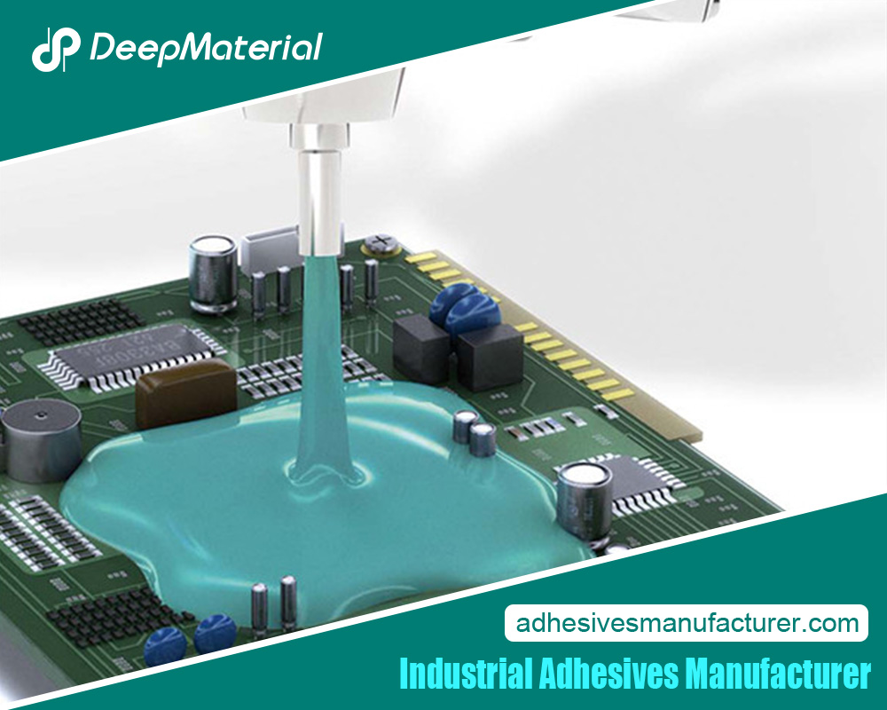
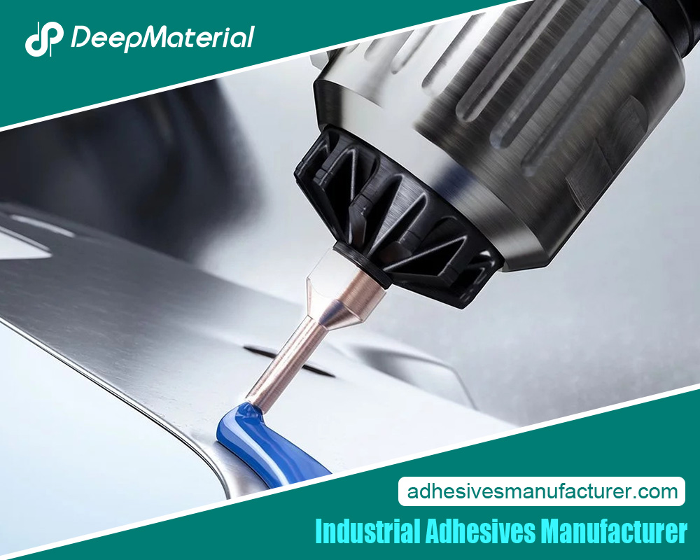
Dispensing and Curing Techniques
Dispensing and curing techniques are critical in various industries, from electronics manufacturing to medical device fabrication. These processes involve precisely applying materials and curing them to achieve desired properties. Here’s an exploration of the key aspects and benefits of dispensing and curing techniques:
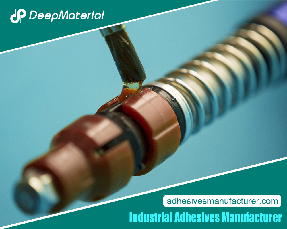
Adhesive Dispensing
- Adhesive dispensing involves precision applying adhesives, sealants, or coatings to specific areas.
- Techniques include manual dispensing, automated dispensing systems, jetting, and needle dispensing.
- Proper dispensing ensures uniform coverage, reduces waste, and enhances bond strength.
Solder Paste Dispensing
- Solder paste dispensing is vital in electronics assembly, applying precise amounts of solder to component pads.
- Techniques like stencil printing, jet dispensing, and laser soldering ensure accurate solder placement for reliable connections.
UV Curing
- UV curing employs ultraviolet light to cure materials like adhesives, coatings, and inks in seconds.
- This rapid curing process enhances production speed, reduces energy consumption, and minimizes heat exposure.
Thermal Curing
- Thermal curing involves using heat to initiate chemical reactions in materials, leading to desired properties.
- People commonly use it for epoxy adhesives, polymer composites, and coatings.
IR Curing
- Infrared (IR) curing uses infrared radiation to accelerate the curing of coatings, adhesives, and composites.
- IR radiation penetrates materials efficiently, promoting uniform curing.
Electron Beam Curing
- Electron beam curing employs high-energy electrons to polymerize and cure materials like resins and coatings.
- It enables rapid curing and offers precise control over the curing depth.
Two-Part Adhesive Dispensing
- Two-part adhesive dispensing involves mixing adhesive components immediately before application.
- Automated mixing and dispensing systems ensure accurate proportions and consistent adhesive quality.
Microfluidic Dispensing
- Microfluidic dispensing uses precision equipment to dispense minute quantities of fluids for medical devices, biotechnology, and electronics applications.
Benefits
- Dispensing and curing techniques ensure accurate material placement, reduced waste, and enhanced process efficiency.
- They enable consistent product quality, improve adhesion, and promote material properties.
Dispensing and curing techniques are indispensable in achieving precise material application and subsequent curing, contributing to the reliability and performance of various products across industries. These techniques empower innovation by enabling the efficient production of intricate designs and complex components.
Quality Control and Inspection
Quality Control and Inspection are critical stages in ensuring the reliability and performance of electronic components, with a particular focus on epoxy underfill encapsulants. These encapsulants protect delicate microelectronics from environmental stressors, mechanical shocks, and thermal cycling. A meticulous inspection process is essential to ensure the highest standards of quality:
- Material Verification:Thoroughly validate the epoxy underfill materials, ensuring they match the specified composition and properties. Consistency in encapsulation is achieved by testing viscosity, curing agents, and filler materials.
- Dispensing Precision:Monitor the dispensing process of epoxy underfill onto the electronic components. This step demands careful control of the dispensed volume, location, and uniformity to prevent voids or excess material.
- Curing Assessment:Inspect the curing process by monitoring time and temperature parameters. Proper curing guarantees optimal mechanical and thermal properties of the encapsulant, contributing to the longevity of the electronic device.
- Visual Inspection:Conduct a visual assessment to detect surface irregularities, air bubbles, or cracks on the encapsulated components. These defects could compromise the component’s performance or longevity.
- Cross-Section Analysis:Randomly sample encapsulated components and perform cross-sectional analysis. This process entails cutting into the enclosed area to inspect the distribution of epoxy and checking for uniformity and voids.
- Adhesion Testing:Evaluate the adhesion strength between the epoxy underfill and the substrate by subjecting samples to stress tests. A strong bond prevents delamination during the component’s operational lifespan.
- Electrical Testing:Verify the electrical integrity of the encapsulated components. Testing examines insulation resistance and capacitance to prevent electrical anomalies caused by the encapsulant.
- Thermal Cycling Tests:Subject samples to thermal cycling tests that simulate real-world temperature fluctuations. This assessment evaluates the encapsulant’s ability to withstand thermal stresses without compromising its structural integrity.
- Reliability Assessment:Perform accelerated aging tests to evaluate the longevity of the encapsulated components under harsh conditions. This process assists in forecasting the performance for an extended duration.
Incorporating these quality control and inspection measures within the epoxy underfill encapsulation process is vital for maintaining the reliability, performance, and durability of electronic components, safeguarding them against the challenges of the operating environment.
Challenges in Application
Epoxy underfill encapsulants play a pivotal role in ensuring the reliability and longevity of semiconductor devices by providing mechanical support, thermal dissipation, and protection against environmental factors. Despite their numerous advantages, addressing specific challenges is necessary to ensure the optimal performance of electronic components when applying epoxy underfill encapsulants.
Challenges and Considerations:
Viscosity and Flow Control
Epoxy underfill encapsulants typically have a high viscosity, making their application challenging. Achieving uniform coverage and proper flow to fill narrow gaps between components is crucial for optimal thermal conductivity and mechanical stability. Balancing viscosity with flow control mechanisms is essential to prevent voids, incomplete encapsulation, and uneven stress distribution.
Curing and Thermal Management
The curing process of epoxy underfill materials involves chemical reactions that generate heat. Effective thermal management during curing is essential to prevent overheating sensitive components and potential damage. Finding the right balance between curing time, temperature, and the encapsulant’s exothermic characteristics is critical to avoid thermal stress and ensure complete curing without compromising device reliability.
Adhesion and Stress Management
Ensuring strong adhesion between the underfill encapsulant, semiconductor die, and substrate is vital for mechanical stability and long-term performance. However, the differential coefficients of thermal expansion (CTE) between various materials can result in stress buildup during temperature cycling. Mitigating stress through proper material selection, design optimization, and controlled curing can help prevent delamination and premature failure.
Compatibility with Advanced Packaging
As electronic packaging technologies advance, incorporating epoxy underfill encapsulants into complex architectures, such as 3D stacked chips and system-in-package (SiP) configurations, becomes more intricate. Ensuring compatibility with these advanced packaging techniques while maintaining high thermal conductivity and electrical insulation requires thorough material characterization and adaptation of application processes.
Quality Control and Reliability
Maintaining consistent quality across mass production of semiconductor devices demands stringent quality control measures. Variations in viscosity, dispensing accuracy, curing conditions, and overall process uniformity can impact the reliability and performance of encapsulated devices. Implementing robust quality control protocols and testing methodologies is essential to detect and rectify defects early in manufacturing.
Innovations in Underfill Technology
In the dynamic landscape of electronics manufacturing, continuous advancements in underfill technology have emerged as pivotal drivers of enhanced device performance, reliability, and miniaturization. These innovations leverage cutting-edge materials, processes, and design considerations to address traditional challenges and unlock new possibilities in semiconductor packaging.
- Nanofillers for Enhanced Thermal Conductivity:Incorporating nanofillers, such as graphene or carbon nanotubes, into underfill materials has significantly improved thermal conductivity. This innovation enables more efficient heat dissipation from sensitive components, reducing the risk of overheating and enhancing overall device reliability.
- Low-Temperature Curing:Traditional underfill materials often require high-temperature curing processes, posing challenges for heat-sensitive components. The development of low-temperature curing underfills allows for more flexible and efficient processing, minimizing thermal stress on the components and substrates.
- Self-Healing Underfills:Innovations in self-healing materials have introduced the potential for underfills to repair minor cracks or defects that may occur during device operation. These materials can autonomously mend minor damages, extending the lifespan of devices and improving their resistance to mechanical stress.
- Flexible and Stretchable Underfills:With the rise of flexible and wearable electronics, underfill technology has adapted to accommodate unique mechanical requirements. Flexible and stretchable underfills offer robust protection and electrical insulation while allowing devices to bend, twist, and conform to various surfaces.
- Additive Manufacturing (3D Printing):Additive manufacturing techniques have revolutionized underfill applications by enabling precise and customizable deposition of materials. 3D Printing of underfills allows for complex designs, reduces material wastage, and supports the realization of intricate packaging architectures.
- Advanced Dispensing and Curing Processes:Innovations in dispensing technologies, such as jetting or multi-nozzle systems, enable more precise and uniform underfill material application. These advancements and optimized curing processes ensure consistent encapsulation quality and reliability.
As the electronics industry continues to evolve, innovations in underfill technology play an instrumental role in addressing the demands of miniaturization, thermal management, and reliability. These advancements empower manufacturers to create next-generation devices that push the boundaries of performance while maintaining stringent quality standards.
Future Prospects and Industry Trends
The realm of epoxy underfill encapsulants is poised for transformative growth as the semiconductor industry continues its rapid evolution. This essential technology, which enhances the reliability and performance of electronic components, is expected to undergo significant advancements driven by innovative materials, process improvements, and changing market demands.
Emerging Materials and Formulations
- Nanocomposite Underfills:Integrating nanomaterials, such as metal oxides and nanoparticles, into underfill formulations hold the promise of achieving higher thermal conductivity and mechanical strength, thus enabling more efficient heat dissipation and prolonged device lifetimes.
- Biodegradable and Sustainable Underfills:As environmental concerns gain prominence, we expect the development of biodegradable and eco-friendly underfill materials to rise. These materials would contribute to reduced electronic waste and support the industry’s sustainability goals.
Advanced Manufacturing Techniques
- Microfluidic Dispensing:Microfluidic-based underfill dispensing systems offer enhanced precision, enabling intricate designs and reducing material waste. This technology is likely to gain traction for next-generation packaging architectures.
- In-Situ Curing and Monitoring:Real-time monitoring and control of the curing process can optimize underfill performance. Innovations in in-situ curing techniques and monitoring sensors will contribute to higher process reliability and yield.
Industry Trends and Applications
- 5G and High-Frequency Electronics:The advent of 5G technology and high-frequency electronics necessitates underfill materials with improved electrical properties and reduced signal loss, driving research and development in this direction.
- Flexible and Wearable Devices:With the increasing popularity of flexible and wearable electronics, underfill encapsulants that offer mechanical protection and flexibility will be in high demand
- Automotive Electronics:The automotive sector’s shift towards electric and autonomous vehicles demands robust underfill solutions capable of withstanding high temperatures, vibrations, and thermal cycling.
Challenges and Considerations
- Reliability and Longevity:As devices become more complex and miniaturized, ensuring long-term reliability through effective stress management, adhesion, and thermal performance remains a critical challenge.
- Standardization and Quality Control:Consistent quality across various manufacturers requires standardized testing methods and quality control protocols to prevent defects and failures.
The future of epoxy underfill encapsulants holds a tapestry of possibilities driven by the synergy of emerging materials, manufacturing techniques, and industry trends. As the semiconductor landscape continues its dynamic trajectory, innovative underfill solutions will play a pivotal role in shaping electronic devices’ reliability, performance, and sustainability across diverse applications.
Epoxy underfill encapsulant represents a remarkable convergence of material science and microelectronics engineering, offering enhanced protection and reliability to the most delicate and advanced electronic devices. Its ability to mitigate thermal and mechanical stresses while facilitating improved heat dissipation has positioned it as an essential component in modern electronics packaging. As technology continues to evolve and consumer demands for smaller, more efficient devices grow, epoxy underfill encapsulant stands poised to play a pivotal role in enabling the next generation of innovative microelectronics applications across industries ranging from healthcare to automotive and beyond.