Potting Compound for PCB: Enhancing Protection and Performance
Potting Compound for PCB: Enhancing Protection and Performance
In the world of printed circuit boards (PCBs), the selection of the right potting compound is crucial for ensuring the reliability, longevity, and performance of electronic devices. Potting compound, a specialized material, plays a vital role in safeguarding PCBs from various environmental factors and mechanical stresses. This article delves deep into the world of potting compound for PCB, exploring its types, properties, applications, and the benefits it offers.
 Introduction to Potting Compound for PCB
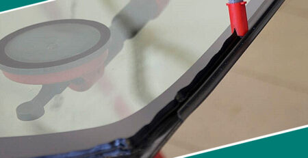
Potting compound is a type of encapsulating material that is used to cover and protect PCBs. It acts as a barrier, preventing moisture, dust, chemicals, and other contaminants from reaching the sensitive components on the PCB. Additionally, it provides mechanical support, reduces vibration, and helps dissipate heat, thereby enhancing the overall performance and durability of the PCB.
Types of Potting Compounds
- Epoxy-based Potting Compounds
Epoxy potting compounds are widely used due to their excellent adhesion, mechanical strength, and chemical resistance. They offer good electrical insulation properties and can withstand high temperatures.
- Silicone-based Potting Compounds
Silicone potting compounds are known for their flexibility, high-temperature resistance, and good moisture resistance. They are often preferred in applications where shock and vibration protection are critical.
- Polyurethane-based Potting Compounds
Polyurethane potting compounds provide a balance of mechanical properties, chemical resistance, and adhesion. They are suitable for a wide range of PCB applications.
Properties and Characteristics of Potting Compounds
- Electrical Insulation
A key property of potting compounds is their ability to provide high electrical insulation. This ensures that there is no leakage of current between components on the PCB, preventing short circuits and electrical failures.
- Thermal Conductivity
Effective heat dissipation is essential for the proper functioning of PCBs. Potting compounds with good thermal conductivity help transfer heat away from the components, preventing overheating and improving the reliability of the circuit.
- Chemical Resistance
PCBs may be exposed to various chemicals in different environments. Potting compounds with high chemical resistance protect the PCB from degradation and corrosion.
- Mechanical Strength
The potting compound should provide sufficient mechanical strength to withstand handling, installation, and operational stresses without cracking or deforming.
Application Areas of Potting Compound for PCB
- Automotive Electronics
In the automotive industry, PCBs are subjected to harsh conditions such as temperature variations, vibrations, and exposure to moisture and chemicals. Potting compounds ensure the reliability and longevity of automotive electronic components such as engine control units, infotainment systems, and sensor circuits.
- Industrial Controls and Automation
Industrial control systems and automation equipment often operate in demanding environments. Potting compounds protect the PCBs in these applications from dust, humidity, and electrical noise, ensuring accurate and uninterrupted operation.
- Consumer Electronics
From smartphones and laptops to home appliances, consumer electronics rely on PCBs protected by potting compounds to offer reliable performance and a long lifespan.
- Medical Devices
Medical devices require high reliability and safety. Potting compounds play a crucial role in protecting the PCBs in medical equipment such as diagnostic devices, surgical tools, and patient monitoring systems.
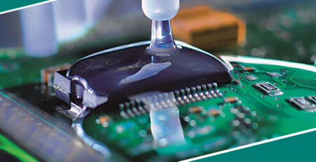
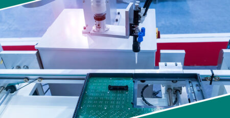
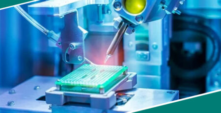
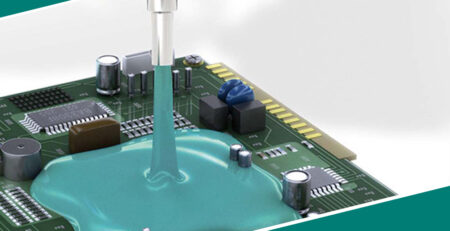
The Process of Applying Potting Compound to PCB
- Preparation
Before applying the potting compound, the PCB is thoroughly cleaned to remove any contaminants or flux residues. The components on the PCB are also inspected to ensure they are properly placed and soldered.
- Mixing (If Required)
Some potting compounds come in two or more components that need to be mixed in a specific ratio to achieve the desired properties. Careful mixing is essential to ensure uniform consistency and performance.
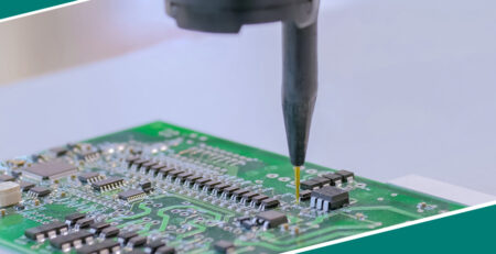
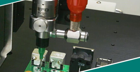
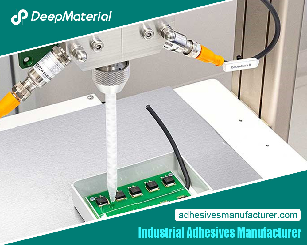
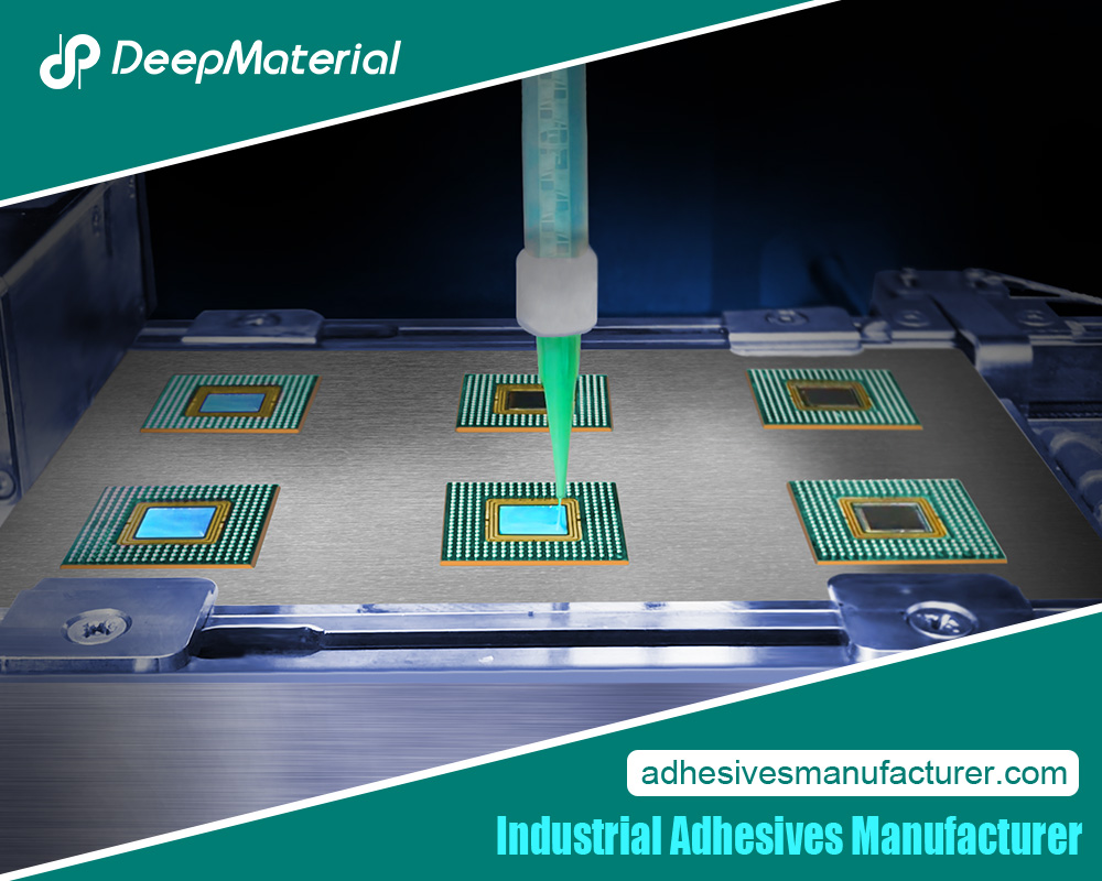
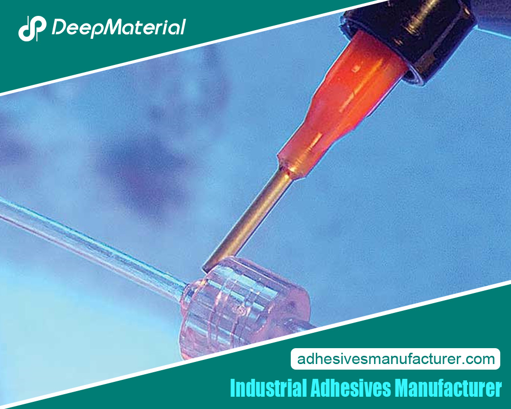
- Application Methods
There are several methods for applying potting compound to the PCB, including pouring, injection molding, and dip coating. The choice of method depends on the size and complexity of the PCB and the production volume.
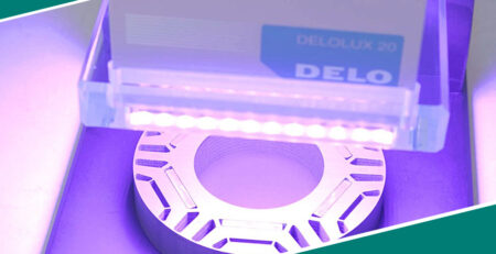
- Curing
After application, the potting compound undergoes a curing process. This can be achieved through heat, UV light, or a combination of both, depending on the type of compound used. The curing time and temperature need to be controlled precisely to ensure proper curing and optimal properties.
Quality Control and Testing of Potting Compound for PCB
- Visual Inspection
The potted PCB is visually inspected for any visible defects such as air bubbles, voids, or incomplete coverage.
- Electrical Testing
Electrical tests are conducted to ensure that the potting compound has not affected the electrical performance of the PCB, such as resistance, capacitance, and insulation resistance.
- Thermal Cycling and Environmental Testing
PCBs are subjected to thermal cycling and exposure to various environmental conditions to simulate real-world usage and verify the durability and reliability of the potting compound.
Advantages and Disadvantages of Using Potting Compound for PCB
- Advantages
- Enhanced Protection: Potting compounds provide a comprehensive shield against environmental factors, mechanical stresses, and electrical interference.
- Improved Reliability: By reducing the risk of component failure and short circuits, potting compounds increase the overall reliability of the PCB.
- Vibration and Shock Resistance: The mechanical support offered by the potting compound helps absorb shock and vibration, protecting delicate components.
- Heat Dissipation: Good thermal conductivity of some potting compounds helps manage heat, preventing overheating and improving the performance of the PCB.
- Disadvantages
- Cost: The use of potting compound adds to the manufacturing cost of the PCB.
- Repair Difficulty: Once potted, it can be challenging to repair or replace individual components on the PCB.
- Weight and Size Increase: The application of potting compound can increase the weight and size of the PCB, which may be a consideration in some applications.
Future Trends and Developments in Potting Compound for PCB
- Development of High-Performance Materials
Researchers are constantly working on developing potting compounds with improved properties such as higher thermal conductivity, better chemical resistance, and enhanced flexibility.
- Environmentally Friendly Options
With increasing focus on sustainability, there is a growing demand for potting compounds that are environmentally friendly, non-toxic, and recyclable.
- Automation and Process Optimization
Advancements in manufacturing processes and automation technologies are expected to improve the efficiency and quality of applying potting compounds to PCBs.
 Conclusion
Potting compound for PCB is an indispensable component in modern electronics, providing essential protection and performance enhancement. The careful selection of the appropriate type of potting compound, along with proper application and quality control, can significantly contribute to the reliability and longevity of electronic devices. As technology continues to evolve, the development of new and improved potting compounds will undoubtedly play a crucial role in meeting the ever-increasing demands of the electronics industry.
For more about a complete guide to potting compound for PCB: enhancing protection and performance, you can pay a visit to Deepmaterial at https://www.adhesivesmanufacturer.com/ for more info.